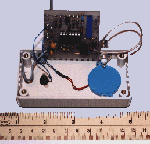
Radio Transmitter

For your comments, suggestions, or your looking for a circuit or design, or a electronics designer, please send you Inquiries to pcb1001@gmail.com. We are happy to help and attend to your concerns.
Showing posts with label RF Application. Show all posts

Friday, June 5, 2009

Active Antenna HF/VHF/UHF, 3-3000MHz

If you have a shortwave or high-frequency receiver or scanner that is struggling to capture signals with a short, whip antenna, and you'd like the kind of performance that a 60-foot 'longwire' antenna can provide but lack the space to put one up, consider building the AA-7 HF/VHF/UHF Active Antenna described in this article. The AA-7 is a relatively simple antenna that is designed to amplify signals from 3 to 3000 MegaHertz, including three recognized ranges: 3-30Mhz high-frequency (HF) signals; 3-300Mhz very-high frequency (VHF) signals; 300-3000MHz ultra-high (UHF) frequency signals. Those bands are typically occupied by shortwave, ham, government, and commercial radio signals.


Active Antennas:

In its simplest form, an active antenna uses a small whip antenna that feeds incoming RF to a pre-amplifier, whose output is then connected to the antenna input of a receiver. Unless specifically designed otherwise, all active antennas are intended for receive-only operation, and thus should not be used with transceivers; transmitting into an active antenna will probably destroy its active components. A well designed broadband active antenna consider field strength of the desired signal (measured in microvolts per meter of antenna length), atmospheric and other noise, diameter of the antenna, radiation resistance, and antenna reactance at various frequencies, plus the efficiency and noise figure of the amplifier circuit itself.


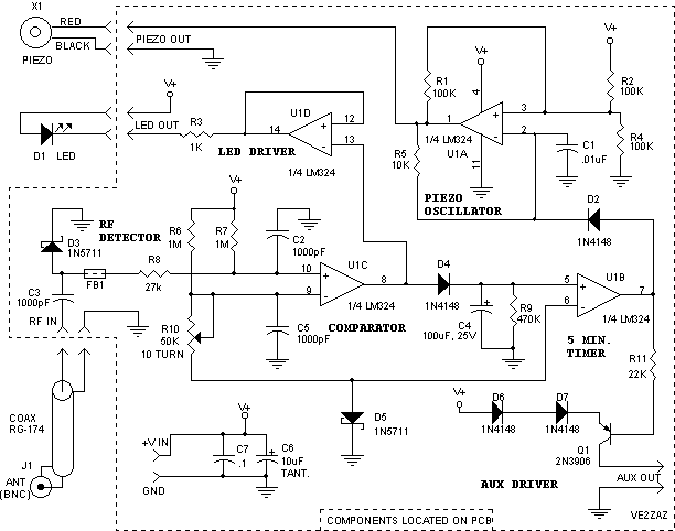
Circuit Description:


Figure shows the schematic diagram of the AA-7, which contains only two active elements; Q1 (an MFE201 N-Channel dual-gate MOSFET) and Q2 (a 2SC2570 NPN VHF silicon transistor). Those transistors provide the basis of two independent, switchable RF pre-amplifiers. Two double-pole double-throw (DPDT) switches play a major role in this operation of the AA-7. Switch S1 is used to select one of the two pre-amplifier circuits (either HF or VHF/UHF). Switch 2 is used to turn off the power to the circuit, while coupling the incoming RF directly to the input of the receiver. That gives the receiver non-amplified access to the auxiliary antenna jack, at J1, as well as the on-board telescoping whip antenna. With switch S2 in its power-on position, the input and output jacks are disconnected and B1 (a 9 volt battery) is connected to the circuit. With switch S1 in the position shown in the schematic, incoming RF is directed to the HF pre-amp circuit built around Q1 (an MFE201 N-Channel dual-gate MOSFET). The HF pre-amp operates with an exceptionally low noise level, and is ideal for copying weak CW and singe-side band signals. When S1 is switched to the other position, the captured signal is coupled to the VHF/UHF pre-amp built around Q2 (a 2SC2570 NPN VHF silicon transistor), which has excellent VHF through microwave characteristics. With the on-board whip antenna adjustable to resonance through much of the VHF-UHF region (length in feet = 234 divide by the frequency in MHz), the VHF/UHF mode is ideal for indoor and portable use with VHF scanners and other receivers. Either mode can be used when tuning 3-30 MHz HF signals. The VHF/UHF pre-amp offers higher gain than the HF pre-amp, but also has a higher noise level. You can easily choose either amplifier for copying any signal; of interest--just try both positions. The RF gain control (R5) can be used to trim the output of either amplifier.

Caution: The AA-7 is not intended for transmitting operation (be it Ham, Maritime, or CB); if it is used with a transceiver of any kind, make sure it is not possible to transmit by accidentally pressing a mike button or CW keyer. Transmitting RF into the AA-7 is likely to ruin one or both of the transistors in the circuit.

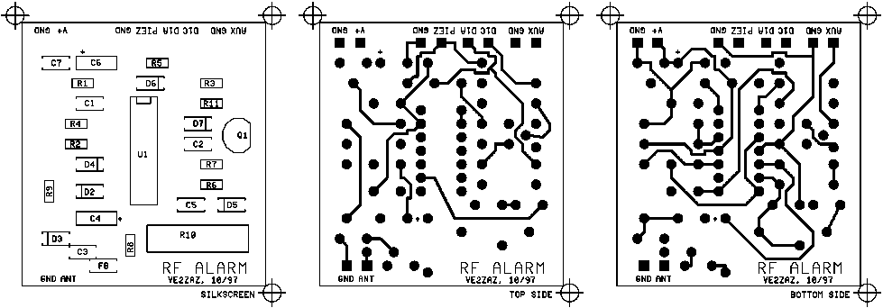
Parts List and other components:

Semiconductors:

Q1 = MFE201, SK3991, or NTE454. N-Channel, dual-gate MOSFET, TO-72 (see text)
Q2 = 2SC2570, NTE107. Silicon RF IF/Amp, NPN transistor (see text)
Note: If you use the NTE107 as a replacement, make sure to insert it correctly
into the pcb. The orientation is different than as shown on the parts layout
diagram. (e-c-b seen front view for NTE107). See this Data Sheet

Resistors:

All Resistors are 5%, 1/4-watt
R1 = 1 Mega Ohm
R2 = 220K
R3,R6 = 100K
R4 = 100 ohm
R5 = 10K potentiometer (pc mount)
Capacitors:

C1,C2,C5,C6 = 0.01uF, ceramic disc
C3 = 100pF ceramic disc
C4 = 4.7 to 10uF, 16WVDC, radial lead electrolytic

Additional Parts & Materials:

B1 = 9-volt alkaline battery
S1,S2 = DPDT PC mount pushbutton switch
J1,J2 = PC mount RCA jack
ANT1 = Telescoping whip antenna (screw mount)
MISC = PCB materials, enclosure, enclosure, battery holder and connector,
wire, solder, etc.

Sunday, May 10, 2009

Radio Spectrum Monitor

This is an experimental work to monitor a spectrum pattern in radio band, and is a continuous project from Audio Spectrum Monitor. To analyze the spectrum of an input signal, I chose an Atmel AVR micro controller that used in the Audio Spectrum Monitor to process FFT. When think it easy, it can be thought that sample an input RF signal directly and analyze it will do. However, you will able to recognize that there are some technical difficulties from following reasons.


  1. The acquisition unit must have a sufficient speed and accuracy that covering over the radio frequency range. As for AM radio band like this project, fast 12 bit ADC and specific controller will able to cover this range. However there is no proper ADC for UHF band.
  2. Number of samples to meet required frequency resolution, fSAMP/fFUND samples, becomes too large. When monitor an AM radio band around 1 MHz in frequency resolution of 500 Hz, over 4000 samples will be required at least. And when monitor a VHF band in same frequency resolution, how many samples will be required...


To solve this difficulties, there is a generic method called Frequency Conversion. In brief, down-convert the RF signal to lower frequency with a mixer (multiplyer) before sampling stage. When process the signals as complex signal for the frequency conversion, it can handle negative frequency, and the center frequency can be moved to zero hertz without interference by image signals. This means that the sampling frequency higher than span frequency range will do. When monitor a 100 MHz band in span of ±1 MHz, it will be converted down to 0±1 MHz and sampled it in only 2 Msps. You may able to understand easy when explain it as `cut and paste' on the frequency domain. Actually, this kind of radio spectrum monitors are being supplied from some radio equipment vendors.

Hardware

In this project, an intermediate frequency signal from mixer output of an AM radio (fC=455kHz) is used as an input signal. It is converted again down to zero hertz in complex signal, so that the signal path, mixer and local oscillator, must be composed for complex signal processing. The complex signal is expressed in two wire IQ signal, the real part corresponds to I signal and the imaginary part corresponds to Q signal. The arithmetic circuits for IQ signal are realized in method of complex arithmetic. For example, a mixing circuit for IQ signals requires four multipliers and two adders from the formula:

(a1+jb1)(a2+jb2) = (a1a2-b1b2)+j(a1b2+a2b1)

Therefore the analog process of IQ signal requires large scale circuit compared to real signal process, so that the IQ signal is usually digitized after minimal analog process and following process are done in digital processor. In case of one input is real, only two multiplyer will do. By the way, when view a real signal as a complex signal, its spectrum pattern of positive part and negative part is line symmetrical. Real signal can be saied that the imaginary part is always zero. The case of complex signal becomes such state is: there are conjugate complex numbers, changed sign of the imaginary part (changed sign of frequency), for each complex frequency components. Therefore the real signal has symmetrical spectrum around the origin.

Software

The firmware samples IQ signal, analyze it in FFT algorithm and draw spectrum pattern into LCD module. These processes are done in refresh rate of approximately 60 times per second. IQ signal is sampled 128 points in samplig rate of 64 ksps at a time, span frequency of ±32 kHz around local frequency (455 kHz) can be monitored. Now horizontal scale (frequency) is labeled on the LCD but when measure local frequency of the radio receiver, the tuned frequency will able to be displayed under the spectrum bars - I became aware this idea during writing this document and implemented it in a hurry:-) When a local input from receiver is valid, frequency scale is appered in the LCD and tuned frequency is refrected.

The fast FFT routine is copied from audio spectrm monitor as is. Basically, FFT algorithm is in complex input/output, it can be used for complex signal with no modification unless it is optimized for real input. When input is a real signal, only half of result is valid because it is symmetrical around the origin. Ofcourse each domain of output is valid when input is a complex signal.

When apply a power, a menu window will apper and can be set working condition with a joystick. Each item can be selected with up/down action, changed with right action and enter running mode with push action. In running mode, up action hold/resume display, down action resets peak hold (if selected), left action redo automatic null (offset cancellation of ADC input) and push action returns to menu. Window function can also be selected, you will able to recognize difference between each window. Wave form mode monitors raw IQ signal but it will not useless.

Free Firmware

Adjustment

  1. Adjust local frequency to 455 kHz with TC1.
  2. Apply 455+10 kHz, 100mVP-P sin wave to the input port and set I and Q signal as same amplitude and quadrature phase at ADC input with VR1 and VR2. And confirm that DC levels are Vcc/2 (a little offset is negligible) and no distortion is recognized.
  3. Enter running mode. When a spectrum bar is 20 bins right from center, it is working successfully. If an image is appering at opposite position, adjust VR1 and VR2 to eliminate it carefully. A peak appearing center at start is due to left DC offset of IQ signal, it will be nulled automatically.

An AM super heterodyne radio receiver is used as a signal source. It may be modified to export mixer output and local oscillator output (this can be ommited). When it is a transister radio, large local frequency component (tuned freqency + IF) will pass through the mixer due to the mixer will be cheap emitter injection type. This affects dynamic range of DBM input, so that unnecessary signals above IF must be filtered out with a LPF. When IF frequency of radio receiver is 450 kHz, please read "455" in this page to "450".

Friday, March 27, 2009

BLV57 Wideband TV Amplifier

Here's the design of BLV57 TV RF amplifier. This construction has been based on a heatsink with a printed-circuit board at the upper side and the bias circuits and a forced air-cooling at the lower side.

PRINTED CIRCUIT BOARD

In the printed-circuit board rectangular holes have been made to mount the BLV57 transistors on the heatsink. For fastening of the printed-circuit board on the heatsink by means of screws, 7 holes of 3.1 mm Æ and for fastening of the hybrid couplers 8 holes of 2.6 mm Æ have been made on the indicated places (see Figs 1 and 2). Hereby has been taken into account the use of Anaren hybrid couplers, type 10264 - 3, suited for the frequency range of 500 - 1000 MHz. Because the 2 bias units have been situated at the lower side of the heatsink, the connections from these units to the circuit take place through the printed-circuit board and the heatsink. For this purpose 9 holes of 2 mm Æ are necessary (4 collectors, 4 bases and 1 ground). To make a good ground contact between the upper and the lower side of the printed-circuit board the following measures have been taken:


  • On 8 spots rivets have been used and soldered at both sides to the metallization of the printed-circuit board. The holes of 2 mm Æ , needed for these rivets, have been situated as indicated in Figs1 and 2.
  • Copper straps with a thickness of 0.2 mm have been soldered at all edges of the printed-circuit board.
  • A good emitter to ground contact has been achieved by soldering 8 copper straps from the upper to the lower side of the printed-circuit board on the spots of each emitter lead.
  • The input connector and the output connector have been screwed to the heatsink but the ground also has been soldered to the printed-circuit board.

HEATSINK

For the BLV57 amplifiers, described in report NCO8101, a blackened heatsink of Seifert Electronic, type KL-117 with a length of 191 mm has been used (see Fig.3). At the lower side forced air-cooling has been applied with a fan trade mark Etri, type 99 XU 01 - 81 with an air displacement of 16 litres per second). By applying this air-cooling the thermal resistance decreased from 0.5 °C/W to 0.2 °C/W.


MECHANICAL MACHINING OF THE HEATSINK

The raised edges at the top side of the heatsink have been removed because the printed circuit board has a width of 113 mm (see Fig.3). To fit the heatsink to the printed-circuit board the following machinings have been carried out:
  • Rectangular holes of 2.8 mm deep have been mould in the heatsink because the transistor leads have to be soldered on the printed-circuit board. Also it was necessary to make avings of 4 mm wide and 0.6 mm deep at the positions of the straps on the printed-circuit board. The transistors have been fastened with M 2.5 screws in the heatsink (see Fig.4).
  • To achieve that the printed-circuit board lays tight to the heatsink also savings have been made in the heatsink on the spots of the 8 rivets through the printed-circuit board.
  • For fastening the printed-circuit board on the heatsink on 7 places, holes with M 3 screwthread have been made in the top side of the heatsink, corresponding with indicated holes in the printed-circuit board.
  • The two hybrid couplers also have been fastened in the heatsink with screws through the printed-circuit board. Therefore 8 holes have been made with M 2.5 screwthread, corresponding with the printed-circuit board.
  • The input and output connectors have been fastened to the heatsink with M 3 screws. The mid contact of each connector makes contact with the printed-circuit board.


UHF Amplifier for TV Transmitter BLV859

Here's TV RF power amplifier circuit for TV transmitter. A broadband linear amplifier design is presented, suitable for application in TV transposers operating in band IV and V (470 to 860 MHz). The design is based on two BLV859 bipolar transistors combined with quadrature hybrids.

Typical results at the recommended class-A bias point (25.5 V/9.1 A) for the total module include 40 W peak sync output power at -54 dB three tone IMD level (fvision = -8 dB, fsound = -10 dB, fsideband = -16 dB) and an average gain of 10.5 dB in the (470 to 860) MHz range.

The BLV859 transistor is a bipolar linear push-pull power transistor designed to operate in the 460 to 860 MHz range. With a specified output power of 20 W peak-sync in class-A it is the largest device in the new generation of transposer transistors. The intermodulation distortion level is < -54 dB (fvision = -8 dB, fsound = -10 dB, fsideband = -16 dB) and power gain;10 dB at 860 MHz. For application in TV transposers for Band IV/V (470 to 860 MHz) a wideband linear power amplifier has been designed with two BLV859 transistors in class-A.

The amplifier consists of 2 balanced circuits (datasheet), both equipped with a BLV859 and oupled in parallel by means of a wideband 3 dB -90 degree sage wireline coupler at the input and output.

For good thermal contact, heatsink compound should used when mounting the transistors on a heatsink.

300mW FM Transmitter 2SC2538

The FM transmitter using a varactor diode way radio, plus a Class C amplifier, RF output power of up to 300 mW more open to more than one kilometer distance communications. Select components: Q1 with ≥ 100 mA, Ft ≥ 300 MHz, β ≥ 100 tubes available 3 DG82, 3DG122, 3DG130, 2G711; Q2 with 2SC2538, 2SC1970, etc..


It must be noted that RF Baffles circle L8, L9, L10; C13, C14, C17, C18, C19, and so can not be omitted, otherwise it would cause unnecessary self-excited oscillation. L1, L5 need to tap extraction, data such as icons, not otherwise due to impedance matching, the output power of less than maximum. Such as a battery-powered, Q3 (Darlington tube), C15, R6 can be omitted. ebugging steps: first in the output termination of testing circuit to regulate the C7, C9, C12 to the largest multimeter readings, remove test circuit connected to one meter in length pole antenna to pull to fine-tune C12 simple reading of the largest field will be completed debugging.

PLL FM Transmitter With BH1415F 500mW

This article is wang1jin (Old: Primary Color love) for the design of RF EDNCHINA.COM FM transmitter board for further analysis, making friends for reference. This EDNCHINA PCB board can be free. Need friends can make reference to relevant websites Learn more.


Designed with PLL technology, BH1415 FM transmitter system block diagram, LCD1602 from STC2052 + + M62429 MIC + + + BH1415 infrared keyboard amplification and high frequency components. (Website procedural reasons, the picture may not clear to the local Save Show)

Microphone FM Transmitter

This is a simple microphone fm transmitter. It operates from a 9V battery as shown above. The old FM mic system was not a perfect solution, so I built this kit and a mixer for the receivers. using three separate transmitter circuits and a mixer on the receiever, the choir voices were perfect and cleanly reproduced.

See detail of microphone FM Transmitter schematic below.


From the notes I made experimentally, C3 is vital to the circuit and without it the circuit may become unstable. C4 is in parallel with C5 and presents a moderate load impedance. Finally all transistors are NPN. The circuit works well and has proved reliable.

In the circuit L1 has 6 turns and has a diameter of 5.5mm and has a length of 4.5mm. Based on the formula for an air cored inductor:

Inductor formula:

Where:
L1 = inductance in uH
r = radius of coil in inches
l = length of coil in millimetres (mm)
n = number of turns on coil

Using the above values, the inductance of L1 can be calculated. A diameter of 5.5mm = 0.22 inches, the radius is half this value or 0.11 inch, the length is 4.5mm and number of turns, n = 6. This gives L1 a value of:


FM Transmitter with 4 Transistors

This circuit is an FM transmitter use four transistors. It provides an FM modulated signal with an output power of around 500mW. The input Microphone preamp is built around a couple of 2N3904 transistors, audio gain limited by the 5k preset.


The oscillator of this fm transmitter is a colpitts stage, frequency of oscillation governed by the tank circuit made from two 5pF capacitors and the inductor. Frequency is around 100Mhz with values shown.

Audio modulation is fed into the tank circuit via the 5pf capacitor, the 10k resistor and 1N4002 controlling the amount of modulation. The oscillator output is fed into the 3.9 uH inductor which will have a high impedance at RF frequencies.

The output stage operates as a class D amplifier , no direct bias is applied but the RF signal developed across the 3.9 uH inductor is sufficient to drive this stage. The emitter resistor and 1k base resistor prevent instability and thermal runaway in this stage.

Voice FM Transmitter Circuit

It is illegal in most countries to operate radio transmitters without a license so take care with transmitter circuits. This FM Low Power circuit may be tuned to operate over the range 87-108MHz band II, with a range of 20 or 30 metres.

Active components in this circuit are BC548 transistors. Although not strictly RF transistors, they still give good results. I have used an ECM Mic (Voice FM ) insert from Maplin Electronics, order code FS43W. It is a two terminal ECM, but ordinary dynamic mic inserts can also be used, simply omit the front 10k resistor. The coil L1 was again from Maplin, part no. UF68Y and consists of 7 turns on a quarter inch plastic former with a tuning slug. The tuning slug is adjusted to tune the transmitter. Actual range on my prototype tuned from 70MHz to around 120MHz.

The aerial is a few inches of wire. Lengths of wire greater than 2 feet may damp oscillations and not allow the circuit to work. Although RF circuits are best constructed on a PCB, you can get away with veroboard, keep all leads short, and break tracks at appropriate points.

VHF/ UHF TV modulator Circuit

Simple TV Modulator that working on VHF UHF Band, the oscillator generates frequency is modulated with the video signal and the modulated carrier wave thus generated is fed into the TV set's aerial input via a cable. Then all that remains to do is tune the VHF UHF TV set to the correct frequency.

Here's TV modulator circuit and see schematic for parts value


The harmonics generator converts the oscillator signal into a sort of frequency spectrum containing all the multiples of 27 MHz up to about 1800 MHz. The TV modulator's output signal is made up of a large number of little peaks, each of which is a complete transmitter signal. At least one of these will always be in band I (VHF channels 2. . . 4), one in band III (VHF channels S. . .12) and many of them will be in bands IV and V (UHF channels 21.. .69).

TV Transmitter Band I and III

This TV transmitter working on VHF Band I and III, using negative sound modulation and PAL video modulation. This is suitable for countries using TV systems B and G, like Australia, Indonesia and Philippines.


This circuit has not been tested at UHF frequencies. The modulated sound signal contains 5.5 -6MHz by tuning C5. Sound modulation is FM and is compatible with UK TV Transmitter System I sound. The transmitter however is working at VHF frequencies between 54 and 216MHz (band I and Band III) and therefore compatible only with countries using Pal System B and Pal System G.

MC1374 TV Modulator

This application note presents the MC1374 TV modulator chip as a suitable device for applications where separate audio and composite video signals need to be converted to a high-quality VHF TV signal.

This TV modulator based MC1374 IC From Motorola with wide dynamic range and low distortion audio make it particularly well suited for applications such as video tape recorders, video disc players, TV games and subscription decoders.

The IC features:
  • Single Supply, 5.0 V to 12 V
  • Channel 3 or 4 Operation
  • Variable Gain RF Modulator
  • Wide Dynamic Range
  • Low Intermodulation Distortion
  • Positive or Negative Sync
  • Low Audio Distortion
  • Few External Components


Stereo Encoder Oversampling For FM Transmitter

Stereo encoder is the circuit that used in FM transmitter audio for a high quality stereo sound transmission. This stereo encoder produces an excellent crystal clear stereo sound and very good channel separation that can match with many more expensive stereo encoders that are available on the market.


Below is stereo encoder (stereocoder) from Katruud Electronic with improved PCB version 3.1. that use 8x oversampling multiplexer method


FM Telephone Transmitter

Here is a simple transmitter that when connected to a phone line, will transmit anything on that line (execpt the dial tone) to any FM radio. The frequency can be tuned from 88 to about 94Mhz and the range is about 200 feet. It is extremely easy to build and is therefore a good, useful beginner project.


Partlists:
  • R1 1 180 Ohm 1/4 W Resistor
  • R2 1 12K 1/4 W Resistor
  • C1 1 330pF Capacitor
  • C2 1 12pF Capacitor
  • C3 1 471pF Capacitor
  • C4 1 22pF Capacitor
  • Q1 1 2SA933 Transistor
  • D1, D2, D3, D4 4 1SS119 Silicon Diode
  • D5 1 Red LED
  • S1 1 SPDT Switch
  • L1 1 Tuning Coil
  • MISC 1 Wire, Circuit Board

Notes
  1. L1 is 7 turns of 22 AWG wire wound on a 9/64 drill bit. You may need to experiment with the number of turns.
  2. By stretching and compressing the coils of L1, you can change the frequency of the transmitter. The min frequency is about 88 Mhz, while the max frequency is around 94 Mhz.
  3. The green wire from the phone line goes to IN1. The red wire from the phone line goes to IN2. The green wire from OUT1 goes to the phone(s), as well as the red wire from OUT2.
  4. The antenna is a piece of thin (22 AWG) wire about 5 inches long.
  5. All capacitors are rated for 250V or greater.
  6. The transmitter is powered by the phone line and is on only when the phone is in use. S1 can be used to turn the transmitter off if it is not needed.
  7. If you have problems with the LED burning out, then add a 300 ohm 1/4W resistor in series with it.


Thursday, March 26, 2009

RF Sensing Alarm


RF sensing alarm is a device that would alert when it detects a continuous RF transmission that lasts more than 5 minutes. The device would have to be broadband (HF/VHF/UHF), be sensitive enough to detect a 5W transmission from inside the shack using a telescopic antenna, and produce a sound loud enough to alert me anywhere in the house.

The RF sensing alarm would also have to be self-contained, which means without any hookups to my radios. After a bit of reading and thinking, I came up with a solution that meets all the initial objectives. Here's circuit in detail.


The circuit shown above may look scary for some of you, but it is not. It can be broken down into four stages. Let's look at them one at a time. The first stage acts as a RF sensor circuit. It is made of U1C, one of the four operational amplifiers of a LM324 chip, and its associated input circuitry. U1C is used as a voltage comparator. Note that the two U1C inputs (plus and minus) have similar DC circuits connected to them. The plus input has R7, R8 and D3, and the minus input has R6, R10 and D5. In these two circuits, D3 and D4 are partly biased (about 200 mV of forward voltage) in order to better exploit the variation of voltage versus current that the diode produces. This translates into increased RF sensitivity.

In an idle condition (no RF detected), potentiometer R10 is set to make the voltage at the minus input of U1C slightly lower then the one at its plus input. This keeps the output of comparator U1C saturated to the "high" state (near supply V+). A strong RF signal present at the antenna terminal J1 reaches D3, a schottky diode, through C3, a coupling capacitor. The diode rectifies this signal and generates a drop of voltage at D3 anode. This makes the voltage at the plus input of U1C fall below the one set at the minus input. As a result, the output of comparator U1C flips down to the "low" state (near ground). In this state, the circuit is in RF detection mode and timer U1B is activated. Note that as soon as the RF signal disappears, the comparator immediately returns to its high state, resetting the entire alarm circuit. Ferrite bead FB1 and resistor R8 are used to block the RF from reaching comparator U1C. Additional RF decoupling is provided by capacitors C2 and C5.

The second stage acts as a timer. It is made of U1B, D4, C4 and R9. U1B is again used as a voltage comparator. When no RF is detected, capacitor C4 is kept charged by the "high" state of U1C. When RF is detected by the first stage, capacitor C4 is left "floating" and starts to slowly discharge through R9. When C4 is sufficiently discharged, after approximately 5 minutes, the voltage at the plus input of U1B falls below the one at the minus input which is set by D5 (about 200 mVDC). As a result, the output of comparator U1C flips down to the "low" state (near ground). In this state, the alarm is tripped. The timer stage drives piezo oscillator U1A and PNP transistor Q1. The latter is added to drive an external device with a voltage close to V+ when the alarm is tripped. The two diodes in series with the emitter provide a drop of voltage so that the base-emitter junction of Q1 is not biased when U1B output is in "high" state. The 2N3906 or equivalent transistor will safely supply a current of up to 50 mA.

The third stage is an astable multivibrator (square wave oscillator) and is made of U1A and surrounding components. It drives the piezo vibrator to produce a loud high-pitch sound. The oscillator circuit will operate only when the output of U1B presents a "low" state. Diode D2 serves as an isolating device between the two stages when U1B is in "low" state. The oscillator's frequency is set by capacitor C1 and resistor R5. The values chosen make the circuit oscillate at approximately 2600 Hz, a frequency that causes the piezo to generate the loudest sound.

The last stage is a simple buffer U1D that sinks current to turn on LED D1 whenever a RF signal is sensed by U1C. R1 limits the current to a safe level for the buffer, less than 20 mA.

The balanced input configuration of comparator U1C allows the supply voltage V+ to vary over a wide range and the entire circuit will still work. I designed the circuit for a 13.8 V supply, but I verified that the circuit works down to approximately 10 V without recalibrating it, and down to approximately 5 V if recalibrated. The high end of the range is more delicate to set since devices such as the LED, the piezo vibrator and polarized capacitors may be overstressed if component value changes are not made. Consequently, I would not recommend going beyond 20 V.

Part Lists

C1 ------ .01uF, ceramic
C2 ------ 1000pF, ceramic
C3 ------ 1000pF, ceramic
C5 ------ 1000pF, ceramic
C4 ------ 100uF, 25V, tantalum or electrolytic (see text)
C6 ------ 10uF, 25V tantalum or electrolytic
C7 ------ .1uF, ceramic
D1 ------ LED, any color
D2 ------ 1N4148 or equiv.
D3 ------ 1N5711, schottky
D4 ------ 1N4148 or equiv.
D5 ------ 1N5711, schottky
D6 ------ 1N4148 or equiv.
D7 ------ 1N4148 or equiv.
FB1 ------ Ferrite bead
J1 ------ BNC, Female panel mount
Q1 ------ 2N3906, PNP or equiv.
R1 ------ 100K
R2 ------ 100K
R4 ------ 100K
R3 ------ 1K
R5 ------ 10K
R6 ------ 1M
R7 ------ 1M
R8 ------ 27k
R9 ------ 470K
R10 ------ 50K, 10-turn pot., Bourns 3006 type
R11 ------ 22K
U1 ------ LM324 Quad Op. Amp.
X1 ------ Piezo, muRata PKM-11 or Radio Shack 273-73 or equiv. External drive type.
Socket --- 14-pin DIP
Coax --- Short piece of RG-174 or equiv.
Box --- Hammond 1591A suggested
Ant --- Right-angle BNC, telescopic

This project is relatively inexpensive to assemble. If all the components are purchased, it should cost less than $25 to build it. Obviously, your junkbox's size will dictate the cost. I re-used components taken from old PCBs. This allowed me to build the project for less than five dollars, including PCB and box.

I admit, it is a rather compact design. The intent here is to make the design fit in a very common Hammond 1591A plastic box. Note that the circuit can be assembled using other techniques: universal PCB, veroboard, deadbug, wire-wrap and even a combination of these techniques. The layout is not critical except for the RF portion of the circuit: Components D3, C3, FB1 and R8 should be mounted as close of possible to each other using very short leads. This will guarantee proper operation up into the UHF spectrum. Also, decoupling capacitors C2 and C5 should be mounted as close as possible to pins 9 and 10 of U1C.

When assembling the PCB, use a soldering iron with a fine tip. Start by installing the LM324 IC. This is the hardest component to solder because of the pin spacing and overall PCB component density. An IC socket is desirable since the LM324 is rather sensitive to pin shorting compared to other operational amplifiers I've used in the past. With a socket, replacing it is a snap. Make sure you solder all components on the two PCB sides. Many component leads are used as vias to jump from top to bottom layers. Soldering all components this way guarantees you a functional circuit at the end. It's happened to me too often to forget to solder a component on the component side of the PCB.

Ferrite bead FB1 is inserted over a short piece of solid wire and the wire is soldered to the PCB pads. Potentiometer R10 is located on the PCB edge so that its adjustment screw can be accessed through a small hole drilled on one of the faces of the box. I've chosen not to put connectors for external connections to the LED, the piezo vibrator, supply line and the auxiliary output. Solder small gauge (#26 or smaller) wires directly to the PCB pads and connect the other ends to the external devices.

For antenna connection, I recommend using a female panel-mount BNC connector. It is small, reliable and will accept most right-angled telescopic antennas when mounted horizontally. Other RF connectors can be used if desired. Since the input impedance of the circuit is quite high, maintaining a constant impedance through the connectors is not an issue. In general though, it is good practice to avoid using UHF connectors (PL-259/SO-239) when working above 200 MHz, since they are not of constant impedance type. For coaxial cable, a short piece of RG-174 type or equivalent is preferred to limit overstressing of the PCB pads. This type of coax is much easier to route in a small box anyway. Solder the bare ends directly to the pads.